RF Receiver General Architecture
Overview
Electronic Warfare (EW) Systems are utilized to control the electromagnetic spectrum (EMS) to attack or prevent enemy operations. EW has been around since the early 1900s and continues to play a pivotal role in wartime strategy. There are three main pillars to EW: electronic attack, electronic protect, and electronic support. Electronic attack (EA) refers to the use of electromagnetic energy to degrade enemy combat capabilities. This could include the degradation of enemy equipment, facilities, or directed electromagnetic attack on personnel. An example of EA would be the deployment of a jammer to degrade enemy communications. Electronic protect (EP) describes the countermeasures taken to defend against an electronic attack. An example of EP would be the use of spread spectrum technology to defend against narrowband jammers. Finally, electronic support (ES) refers to the detection/surveillance of electromagnetic energy. The goal of ES is to identify possible threats in the immediate environment. ES capabilities enable battlefield commanders to make decisions and prioritize responses to these detected threats.
Electronic support – and more specifically the testing of ES receivers – is the main topic of discussion within this course. ES provides immediate threat warning information in oftentimes contested and congested military environments. The outcome of the course will be to provide learners with the knowledge and skills necessary to test and validate EW receiver systems. As one might expect, a strong basis in RF technology will be required to ultimately grasp the skills needed to effectively test these systems. The first module will discuss the fundamental characteristics of an RF receiver analog front end and its associated measurements. Then the course will move on to the digital back end of the receiver where a series of signal processing techniques are employed. Measurement/validation of the standalone digital subsystem will be discussed in this module. The third, and final, module will describe full system-level testing of an EW receiver.
How does a receiver system work?
On a fundamental level, an RF receiver system senses electromagnetic (EM) waves in the RF region of the electromagnetic spectrum, and extracts the information carried by the RF wave into usable information. This useable information could be the sound of someone’s voice, the opening of a keyless car door, or the active threat information provided by an EW receiver. The receiver consists of three main components: a front-end antenna, an analog RF front end, and a digital backend.
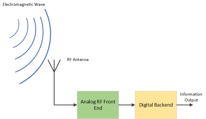
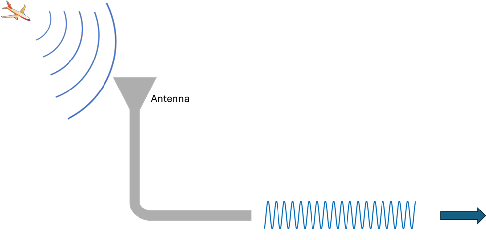
The antenna is a conductive material with a specific geometry and material property which can convert a travelling free-space electromagnetic wave into an electrically conducted wave, and vice versa. The antenna is a passive component which feeds the captured RF wave into the analog front end of the receiver system. Some modern antennas are now active devices, but for the purposes of this discussion we will consider all antennas to be passive devices.
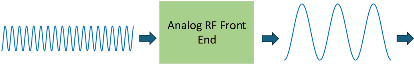
The analog RF front end consists of a series of components which take in RF signals conducted by an RF transmission line. The RF front end conditions the input wave such that the digital backend can process the RF energy. In many situations the front end down-converts the frequency of the input RF wave into a lower frequency. This down-conversion places the frequency of the signal at frequency low enough for the digital backend to process. The front end also amplifies and filters out unwanted signals in the RF spectrum which do not carry relevant information to the task at hand. This will become clearer in subsequent sections of the course.
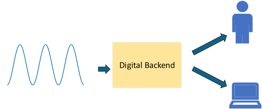
The digital backend of the system converts the analog RF signal into a digital representation of the signal. The backend then extrapolates information of the input signal and presents the data into a useable format for a human or another digital system.
It is important to point out that the receiver system requires a cooperation between the specifications of each subsystem. If the antenna operates at a frequency range outside of the frequency range of the RF front end, the system won’t operate as planned. If the output frequency from the RF front end is too high and outside the analog bandwidth of the analog-to-digital converter on the backend, again the system won’t operate as planned. Careful planning of the full system design is necessary to ensure the receiver operates in the correct frequency range, bandwidth of interest, and power level. In the next few sections we will dive deeper into the operation of each of these subsystems.
Antennas
As discussed in the previous module, antennas provide the backbone for converting free space signals into conducted signals which the RF system can electrically process. Antennas come in all shapes, sizes, and materials. The physical properties of an antenna provide the system designer with the antenna pattern such that the integrator knows the best position to place the antenna for optimal signal reception.
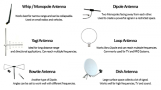
There are tradeoffs to each antenna specific to each application. For example, an isotropic antenna has equal antenna reception strength in all directions in three-dimensional space. Truly isotropic antennas do not exist in reality, but antennas such as dipole antennas provide similar properties. This could be useful for an application where signal strength is not a problem, where it is important to keep cost low and where the received signal could come from any direction. On the other hand, a highly directed antenna would be required for an application with requirements to optimize the signal to noise ratio and with access to fine pointing capabilities toward the transmitted source.
To keep the concepts in this module simple, a discussion of Maxwell’s equations will be skipped. Nevertheless, Maxwell’s equations provide the basis to all higher-level antenna specification equations. In this section we will focus on polarization, directivity, gain, and input impedance.
Polaraization
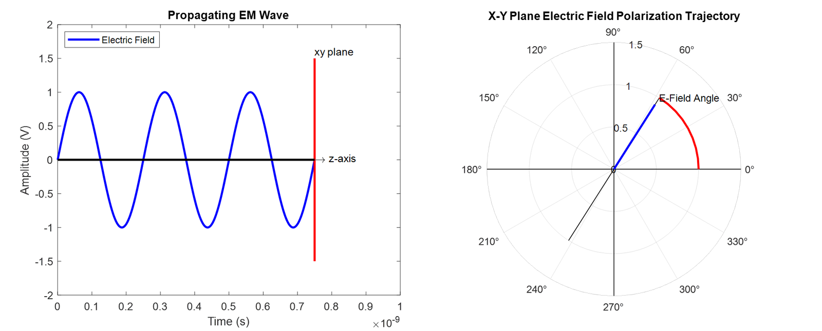
The polarization of an EM wave is the 2-dimensional trajectory of the magnitude of the electric field in the plane perpendicular to the EM wave’s propagation direction. For example, as an EM wave propagates in the z direction, the trajectory of the tip of the electric field in the x-y plane is the polarization. In the case of a linearly polarized wave, the E-field oscillates linearly at any angle in the x-y plane. On the other hand, a circularly polarized wave rotates around the z axis in the x-y plane.
Directivity and Gain
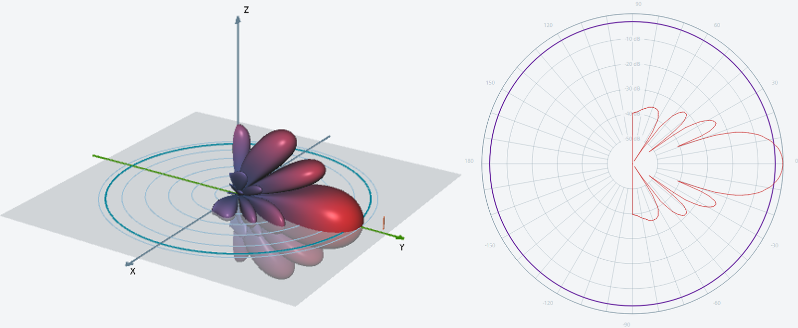
The directivity of an antenna refers to the maximum radiation intensity of an antenna in its main direction relative to an ideal isotropic radiator with the same radiated power. Higher directivity antennas provide more receive/transmit strength in a given direction. In practice, antennas have antenna feed ports to connect to a conducted transmission line. The connection to the feed port often results in an inefficiency relative to the ideal radiated power of the antenna. The gain of an antenna takes this inefficiency into account by measuring the input power to the antenna and capturing the radiated power at the transmitted output in free space. This describes the transmit case for an antenna, although the receive case is identical. Therefore, the antenna gain is defined as the maximum radiated power of an antenna relative to an isotropic radiator with the same input power. The gain is a measurable value which is more practical and is therefore discussed more often in an engineering setting.
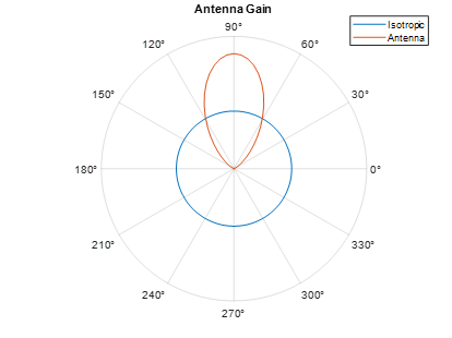
The antenna gain is often measured in dBi which is the radiated power relative to the isotropic radiator in dB.
Analog RF Front End
The analog RF front end consists of a series of components which condition the input RF signal coming from the antenna to drive the digital backend of the system. The conditioning of the signal often requires filtering, amplification and frequency conversion to provide a clean output signal. We often call the frequency to which the RF signal is converted the IF signal. IF stands for intermediate frequency. The IF is chosen to accommodate the analog-to-digital (ADC) analog bandwidth on the digital backend. ADCs will be discussed in the next module. This module will cover the operation and interaction between the three main components of the analog front end: filters, amplifiers, and mixers.
Filters
RF filters are used to perform what the name implies. Filters remove unwanted power coming from signals outside of the receiver’s required bandwidth. Every RF component has a frequency response which impacts the amplitude and phase of an RF signal over a specific frequency range. A filter is designed with the specified intent to impact the magnitude and/or phase over the intended frequency range.
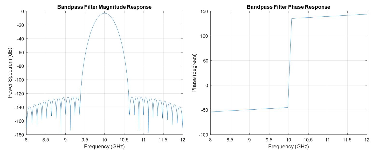
In the example shown here, the filter is designed to remove signals outside of the 10GHz range. If we take a closer look at the magnitude response scale on the y axis, the filter reduces the magnitude by 6dB lower than 9.9GHz and above 10.1GHz. Therefore, the passband of this filter is the range between 9.9GHz and 10.1GHz. Any signal within this range is fed through the system, while signals outside of this range are filtered out.
Amplifiers
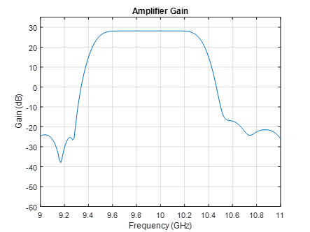
Amplifiers boost the input signal magnitude such that the components downstream from the amplifier have a stronger signal to process. A typical amplifier has a few key characteristics: gain, frequency range, P1dB compression point, noise figure. The gain is the of ratio of output to input power often expressed on the dB scale. The frequency range is the range over which the amplifier operates. The gain is a frequency-dependent parameter which can be displayed as a frequency response over the range of interest.
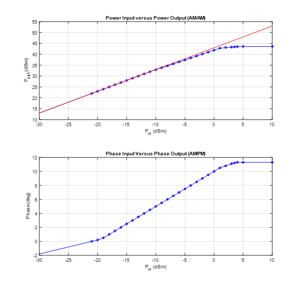
Another important consideration in amplifier design is compression. A linear amplifier is designed to provide the same gain over a range of input power levels. For example, an amplifier designed for 42dB of gain will provide 42dB of amplification if the input power is -30dBm or if the input power is 0dBm. Nevertheless, there will eventually be a limit to how much output power the amplifier can produce. As the input power is increased, no more output power can be produced. We call this compression. The diagram displays the theoretical continuously linear red curve, whereas the blue curve provides the actual input versus output power of the amplifier. As the input power increases, the output power eventually compresses to a saturated power region. The point at which the two curves deviate by 1dB is considered the P1dB compression point. For communication receiver systems, amplifiers are often specified to operate in the linear region of the curve to avoid distortion effects produced in the saturation region.
Additionally, all amplifiers produce a phase change at the output relative to the input phase of the RF signal. This phase change is reflected in the lower plot referenced to the signal input power. Phase changes can result in delay distortion especially in the case of wideband signals. The group delay concept will not be covered in this module.
Another important concept in RF amplifiers is noise figure. Noise figure is the degradation of the signal-to-noise ratio between the amplifier input and output referenced to a 50Ω input and output impedance. The concept of impedance will not be covered in this module, but the main idea is that the electronics in RF amplifiers add noise to the signal at the output. The goal of any receiver system design is to minimize the amount of noise added to the signal at the output. The more noise present at the output of the analog RF front end, the more difficult it becomes for the digital backend to process the signal accurately.

Frequency Converting Mixers
The basic concept around frequency conversion goes back to a series of fundamental trigonometric functions. RF Mixers are three-port devices which multiply two input signals to produce an output signal at a different frequency. RF signals are composed of a series of sinusoidal waves. If we multiply two sinusoidal waves, we produce a new sinusoidal wave with the following equation:
cos(x)cos(y)=0.5[cos(x-y)+cos(x+y)]
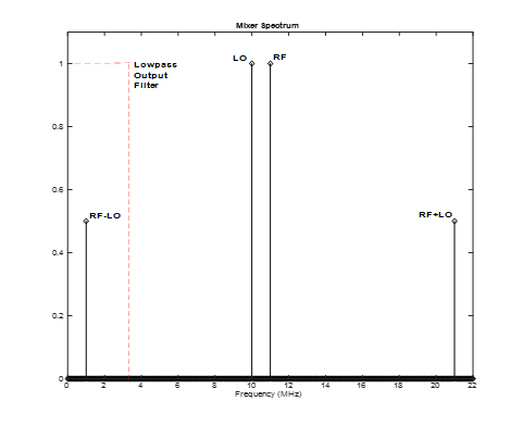
This function tells us that two sinusoidal signals multiplied together result in an output signal composed of two signals: one signal with a frequency that is the sum of the two input frequencies and one signal with a frequency that is the difference of the two input frequencies. For example, if one were to multiply a 10MHz signal with an 11MHz frequency, the output signal would consist of a 1MHz signal and a 21MHz signal. The mixer also produces additional signals which are the sum/difference products of harmonics of the two input signals. Nevertheless, for the purposes of this discussion, the primary sum and difference products will be considered. In the case of a receiver, the output 1MHz signal will be useful to drive the digital backend of the system at a lower frequency than the input 11MHz RF signal. By applying a filter after the mixer which rejects frequencies above 1MHz, the digital backend processes a clean 1MHz copy of the input 11MHz RF signal. This is a fundamental example at a lower frequency, but the concept carries through to higher frequencies.
Mixers define the signal applied and produced as the RF signal, the local oscillator (LO) signal, and the IF signal. In the receive case, the RF signal is mixed with the LO signal to produce a lower frequency IF signal. In the transmit case, the IF signal is mixed with the LO signal to produce a higher frequency RF signal.
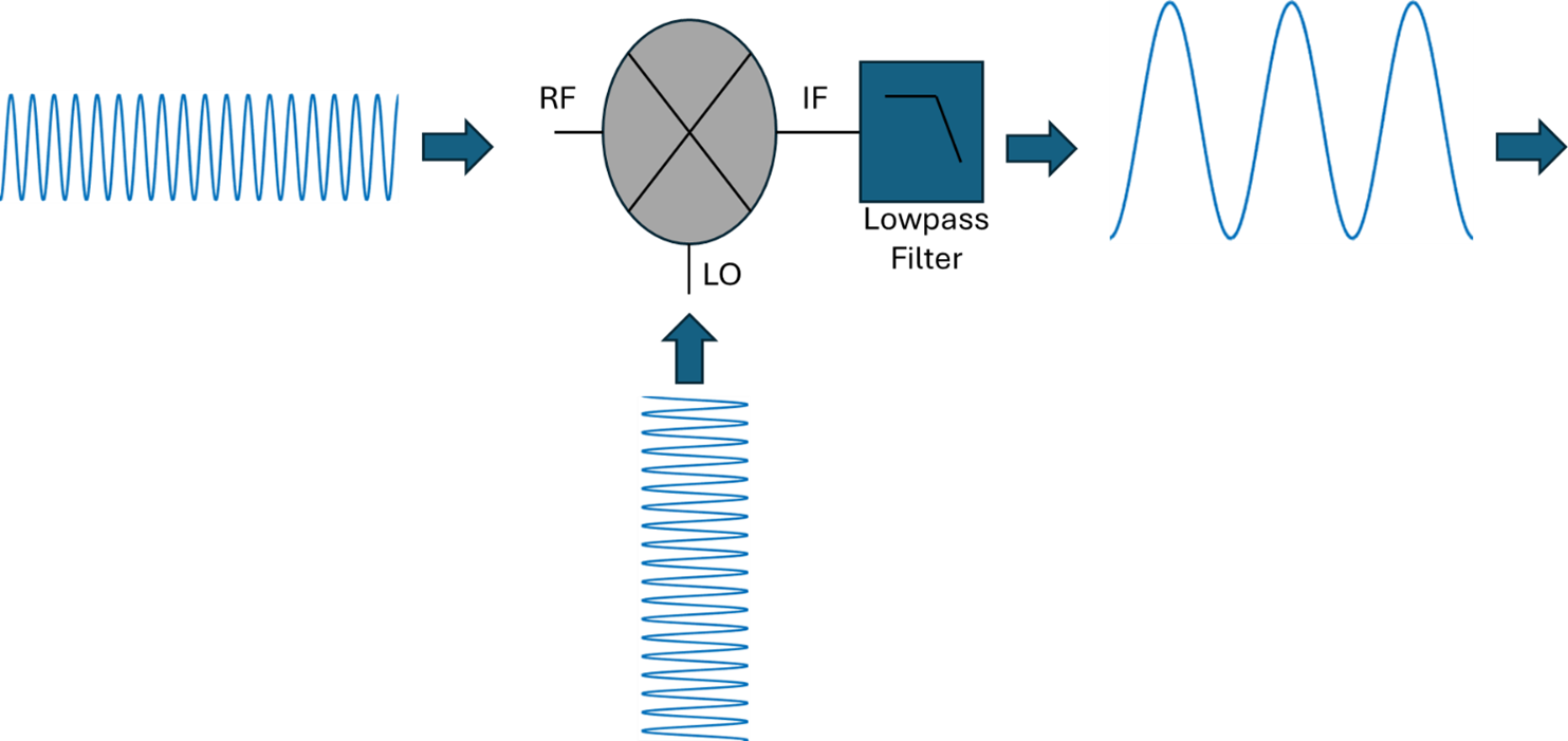
Cascaded Architecture
By concatenating a front-end filter with an amplifier, mixer, and lowpass output filter, the input RF signal can be down converted to an output signal with the proper frequency and level for the digital backend to process.

The next module will discuss the analog to digital conversion process, as well as the different signal processing techniques which can be applied to the received signal.
Digital Backend
The digital backend of a receiver consists of an analog-to-digital converter (ADC) and a digital signal processing (DSP) system which can operate on digital data. This may include a CPU, an FPGA, a GPU, or some type of dedicated digital signal processing (DSP) unit.

Analog-to-Digital Converter (ADC)
The ADC is a critical component in every modern RF receiver. It converts the input IF signal to a digital representation of the signal. On a fundamental level, an ADC samples the input signal and converts the sample into a numerical value representative of the amplitude of the signal at the time the sample was captured. The ADC samples the input signal at a constant clock rate such that a new sample is presented to the output of the ADC at every clock tick. Sample rate will become an important factor in specifying the ADC.
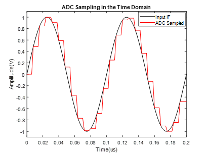
As it becomes more apparent, the sample points on the curve are sufficiently close together to resolve the input signal. The closeness of the sample points constitutes the sample rate. The higher the sample rate the closer the points are together, and therefore the higher the resolution of the output digital signal. Keeping this concept in mind, if the sample rate is too low the output digital signal may not have sample points sufficiently close together to resolve the input signal.
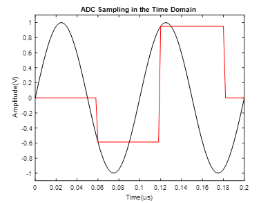
Digital signal processing theory presents the Nyquist sampling theorem which states that any RF signal must be sampled at a rate of twice the highest frequency component of the input signal. Sampling at the Nyquist rate ensures that no aliasing will occur at the digital output of the system. Aliasing refers to the overlapping of frequency components in the RF spectrum which result in indistinguishable mixing of these frequency components after sampling occurs.
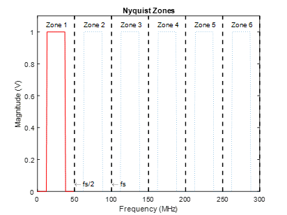
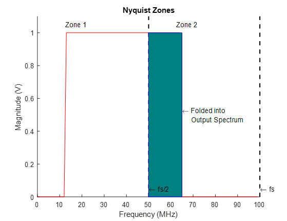
The Nyquist zone plot displays the captured RF spectrum zones presented at the output of an ADC sampled at 100MHz. It is important to point out that any RF energy within any zone will mix with the RF energy in the first zone. For example, an RF signal at which spans 12.5MHz to 65MHz contains energy in both Zones 1 and 2 when the sample rate of the ADC is 100MHz. The signal from 50MHz to 65MHz will fold into the 0 to 15MHz portion of the output spectrum resulting in an aliased signal. This is why receiver designers often put an anti-aliasing filter prior to the ADC input. The ani-aliasing filter removes unwanted signals outside of the main Nyquist zone to avoid the aliasing effects.
It is often discussed that the ADC is sampled at a rate of twice the maximum frequency component of the input IF signal. Based on the Nyquist zone concept discussed in this section, one can deduce that it is also possible to design the input IF signal frequency to fall within the center of a Nyquist zone other than Zone 1. In this case, a bandpass anti-aliasing filter must be applied around the desired IF signal. Higher IF signals can be desirable for image rejection purposes, which will not be discussed in this section. Nevertheless, the designer must ensure that the ADC analog input bandwidth can handle the higher IF frequency above the sampling frequency of the ADC. This architecture is often described as a subsampled receiver.
Digital Signal Processor
A digital signal processing (DSP) unit takes in sampled data from the ADC representing the original analog IF signal. It is the job of the DSP to perform calculations on the input signal to extract the desired information from the signal. The DSP may be responsible for demodulating and decoding an input communication signal, operating on a pulsed radar signal, performing spectroscopic measurements, or conducting any other operation commonly performed on RF signals. Depending on the application, the DSP will contain a series of different processing blocks to accomplish the task at hand. In the case of an electronic warfare receiver, the processing may consist of a filter bank, pulse processing block, an emitter classification block, and a series of higher level operating procedural blocks. Details on the internal structure of the DSP will not be covered in this module.