Electronic Warfare Signal Genration Test Systems - The RF Front End
Within the radar and electronic warfare RF test environment, there are a variety of test & measurement necessities ranging from fundamental component tests to full system-level EW receiver validation tests. One of the key technologies required for EW receiver system-level testing is a signal generation system capable of emulating a realistic RF environment. In a real-world battlespace environment, there are often many signals stimulating the EW receiver. Cluttered RF environments pose challenges to the EW system to make proper decisions between battlefield threats and benign signals. The goal of an EW stimulus test system is to provide the closest representation of a congested RF environment as possible.
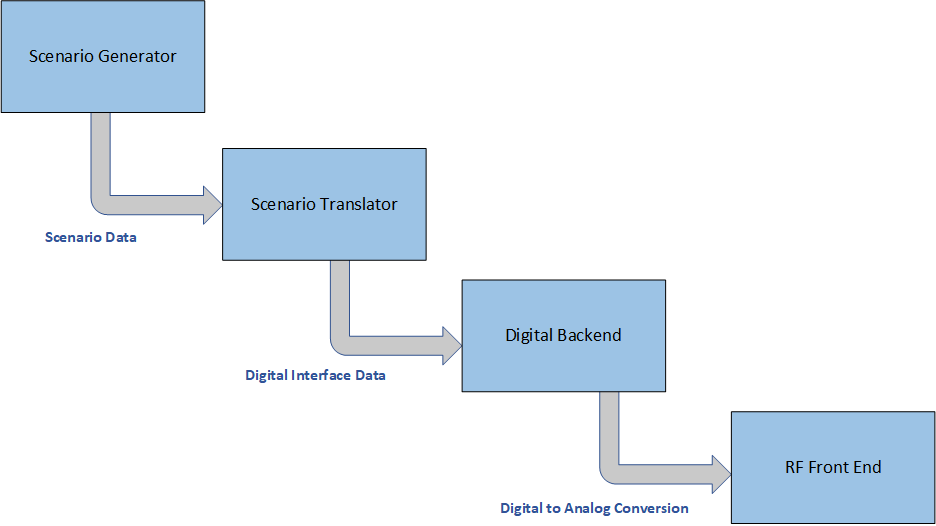
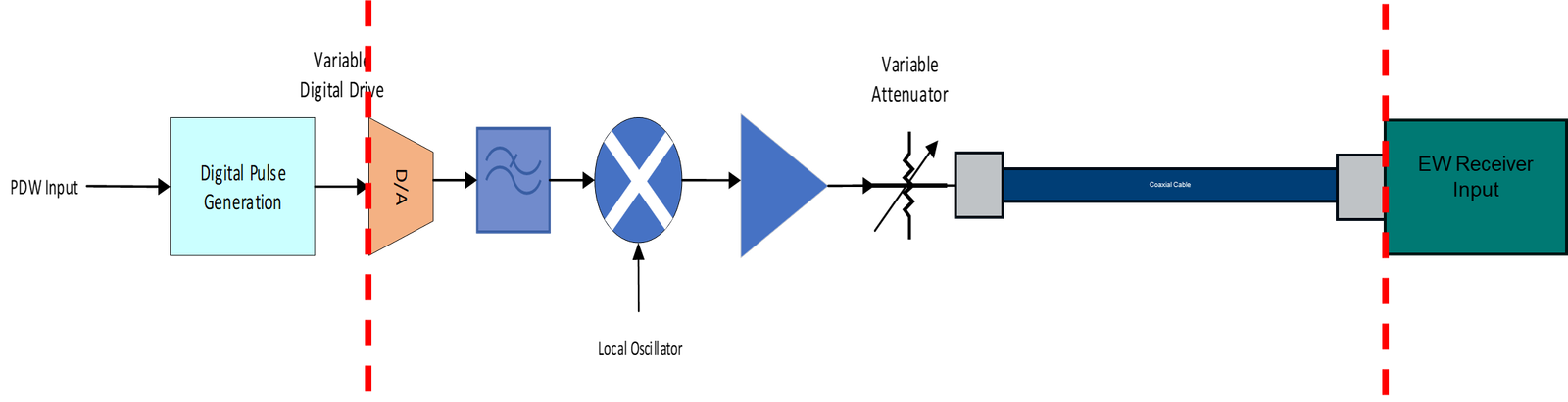
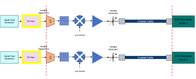
In considering the building blocks of a signal generation system capable of emulating an EW environment, it is important to begin by understanding the test necessities of the EW receiver being tested. The RF requirements of the receiver often include general specifications such as frequency range, instantaneous bandwidth, and dynamic range. If the receiver expands to multiple antenna ports with interferometric or TDOA capabilities, the specifications expand to include port-to-port phase, amplitude, and time alignment tolerances. The hardware complexity on the signal generation test system side of the equation increases with the upward trend in receiver capabilities.
Moving to the next layer of the EW signal generation test system architecture, one must understand the capabilities of the digital interface driving the RF front end. Recall that the overarching goal of the test system is to provide the receiver with the closest representation of a real-world RF scenario. A digital backend subsystem capable of driving high rates of RF pulses over a wide instantaneous bandwidth has significant advantages over less capable systems. Higher pulse rate capacity on the digital backend enables the user to generate scenarios with higher pulse rate emitters or - more importantly - scenarios with more simultaneous emitters in the environment. On the same token, wider bandwidths fundamentally enable the test system to emulate wider bandwidth signals in the scenario. Different radars produce different bandwidth signals for pulse compression purposes. The best test system will be able to emulate the widest emitters in the battlespace.
In the third layer of the architecture, there is a converter to bridge the gap between scenario information and the digital backend. The tool needs to be able to ingest scenario information containing emitter locations within a particular environment and to translate that information into the language that the digital backend can read. The converter block provides the link between the operator and RF.
Finally at the highest level of the architecture, the scenario generation tool enables a user to build up emitters and to tie those emitters to physical platforms that can be placed on map. Emitters are defined with specific pulse widths, pulse rates, modulation types, bandwidths, modes of operation, antenna patterns, antenna scans, and power levels. Emitter definitions can become highly detailed, and many intelligence communities have compiled classified sets of databases containing detailed emitter definitions from various threat environments. The scenario generation tool is critical to setting up a particular test scenario in a human-readable format.
In designing a system architecture that closely satisfies the goal of generating the most realistic RF environment, it is important to understand that the capabilities and specifications of each subsystem are interlinked. For example, an RF front end which can switch frequencies in very short periods of time may offload some of the bandwidth requirements on the digital backend. The critical details will be discussed in the dedicated sections hereafter.
RF Front End Architectural Tradeoffs
The RF front end of an EW environment emulator has a series of specifications that the designer must consider in the effort to provide clean and accurate signals to the EW receiver under test. This module will discuss those specifications in detail.
Frequency and Dynamic Range
The most fundamental specification on any signal generator is the frequency range. To be able to emulate various emitters at various frequencies in the RF environment, the generator must be able to cover the full range of expected frequencies seen by the receiver. More specifically, it needs to be able to match the frequency range covered by the receiver.
Additionally, the dynamic range of the generator needs to cover the dynamic range of the receiver as closely as possible. For example, if the receiver can measure power levels down to -100dBm and up to 0dBm, the generator would ideally be able to cover this exact power range or more. If the dynamic range of one generator cannot comply with the receiver specifications, the architect could conceivably use two combined generators with attenuation on one generator output. Nevertheless, a designer aims to keep size, weight, power, and cost (SWAPC) low, and adding more hardware degrades the SWAPC.
Spur-Free Dynamic Range
One of the key metrics in evaluating the performance of an EW signal generation test system is the spur-free dynamic range. The spur-free dynamic range (SFDR) is the difference in power level between the wanted signal and the highest spur within the specified bandwidth of the test system.
Bandwidth and RF Switching Speeds
When it comes to specifying the bandwidth of the signal generator, certain terms and particular topics need to be discussed to fully understand the problem. Recall the overarching goal of the EW environmental emulator: to provide the most realistic set of signals to the receiver under test. If the receiver is continuously monitoring a particular frequency range, then the generator would ideally be able to produce signals at any frequency in this range without any unwanted gaps over time or frequency. This concept becomes a challenge when real hardware is at play. The following subsections will define key concepts and provide background to the architecture challenges associated with the RF front end design of an EW generation test system.
Instantaneous, Modulation, and Hopping Bandwidth
It is important to begin by defining the key terms referred to in the subsection header: instantaneous bandwidth, modulation bandwidth, and hopping bandwidth. These three terms can sometimes become conflated, and it is crucial to draw a distinction between them.
Instantaneous bandwidth refers to the bandwidth that the EW receiver is continuously monitoring. For example, the receiver may have a continuous view of 2GHz of bandwidth. Any signal within the 2GHz of bandwidth centered at a specific frequency will be captured by the receiver for processing on the backend.
Additionally, the receiver may have multiple channels with multiple different instantaneous bandwidths centered at different frequencies in the spectrum. In this case, the generator needs to be able to cover any – and ideally all – signals within all the receiver bands.
Modulation bandwidth refers to the bandwidth of specific signals within the instantaneous bandwidth of the receiver. The receiver itself may have 2GHz of instantaneous bandwidth, but the radar signal it is seeing at a particular instant in time may have only 30MHz of modulation bandwidth. This is an important consideration for the generator design. The generator RF signal bandwidth may not need to match the receiver instantaneous bandwidth. If the generator can cover the maximum modulation bandwidth of any given signal, and it can retune its center frequency within the instantaneous bandwidth of the receiver, then the system is accurately representing the scenario as desired. Although there are tradeoffs to this, which is where hopping bandwidth comes into play.
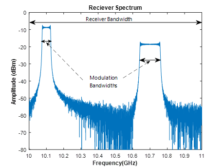
The hopping bandwidth of the EW test generator describes the bandwidth over which the generator is capable of quickly moving it’s center frequency. The term “quickly” is critical in this case, as the speed with which the generator can retune it’s center frequency dictates how accurately one can represent a realistic scenario. If the generator has the capability to quickly “hop” from one pulsed signal to another, and the two pulse signals are not active at the exact same time, then the generator can create intermittent signals that are apparently simultaneous to the EW receiver. The generator needs to be able to retune the center frequency very quickly to avoid missing moments in time when one of the signals needs to be active. If the retune time is too slow, certain pulses may be dropped from the scenario which would degrade the realistic nature of the receiver’s viewing window.
Overcoming the Simultaneous Emitter Problem
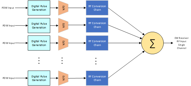
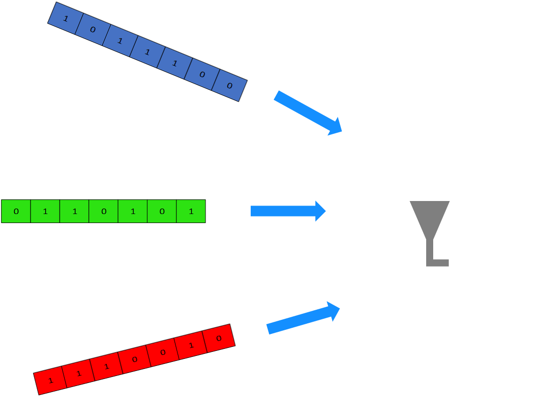
The hardware problem becomes clearer as one begins to recognize that simultaneous emitters are difficult to generate on a single signal generator port. If the EW test scenario calls for N simultaneous emitters within the receiver instantaneous bandwidth, then the goal of the signal generator test system is to produce N simultaneous signals on a single input to the receiver.
As discussed, the generator can emulate multiple simultaneous signals by hopping back and forth between emitters as they become active. But if multiple signals are active at the same time, then only one signal can be assuredly generated. This is not ideal from a test perspective, although some would argue in favor of the “good enough” principle. Not every test will need to perfectly emulate every signal in the receiver bandwidth, but rather the most important signal at any instant in time. This is where prioritization comes into play. Some emitters can be classified with higher priority over others in a test environment with limited hardware resources. Higher priority emitters take precedent over lower priority emitters. In this test scheme, the hopping generator will always hop to the highest priority signal even if there are multiple lower priority signals simultaneously active in the scenario.
Prioritization is one solution to the multi-emitter problem, but it begins to fall short as the test scenario becomes highly dense. More simultaneous signals lead to more dropped pulses on a single generator RF port. The most obvious solution to improve the pulse density is to add more signal generators and to combine their outputs through an RF combiner into one receiver port. Although before discussing the combinatorial approach, there is another approach in modern wideband vector signal generators.
Wideband vector signals generators (VSG) operate as the name implies: they produce RF signals over a wide instantaneous bandwidth. Wideband VSGs equipped with an arbitrary waveform generator (AWG) can produce pre-calculated IQ baseband waveforms that span the full bandwidth of the VSG. If the user has a priori knowledge of the full scenario, then multiple emitters can be constructed from a single IQ file played out on a single RF port. The problem often comes to the memory depth inherent to the AWG. Limited memory depth results in shorter file limits, and therefore reduced scenario playout times – especially with wider spacing between emitters (i.e. wider utilized AWG bandwidth). A full analysis of AWG memory depth and bandwidth limitations will not be covered in this discussion.
Assuming the EW scenarios are long, and that the scenarios take up a wide bandwidth, combining multiple signals provides the most intuitive approach to the multiple emitter problem. The following subsections will discuss two architecturally different mechanisms for combining multiple emitter signals.
Analog Domain Combination
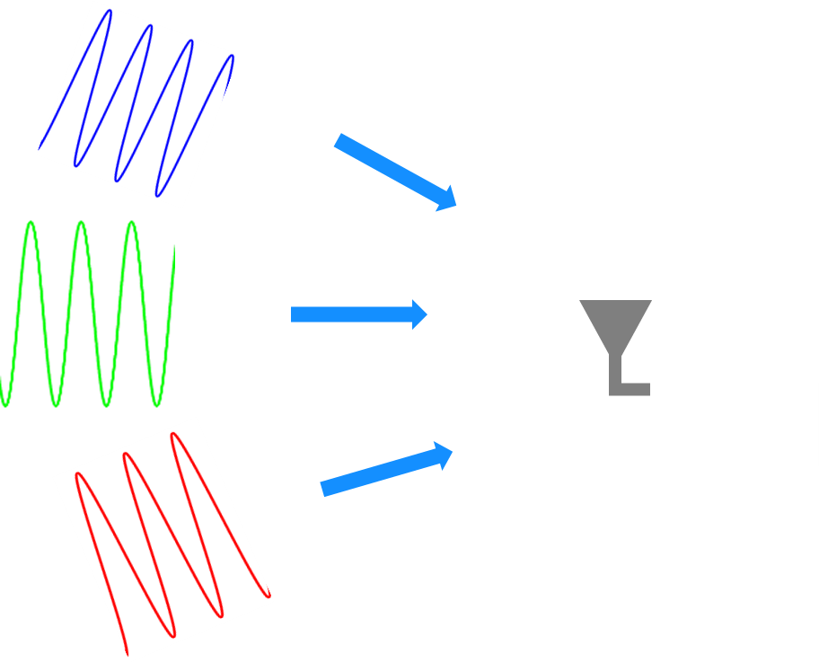
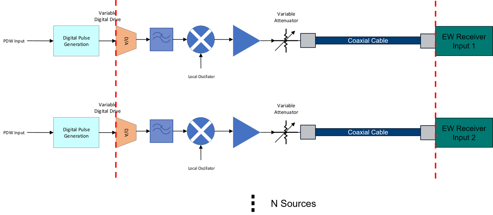
One way of generating test scenarios with multiple simultaneous signals is to combine multiple signal generator ports with an RF combiner. There are many advantages to this approach. One major advantage is that every independent signal generation source can tune to any frequency within the frequency coverage of the receiver. Additionally, every source’s RF front end can have a settable power level by modifying the source’s amplification/attenuation settings. This provides more dynamic range compared to a digitally combined approach, which will be discussed in the next section.
The figure above provides an architectural diagram of the multiple-source approach. One of the major drawbacks of this architecture is that the SWAPC can grow exponentially as requirements on pulse density are increased – especially when multiple receiver ports become involved. The multi-port discussion will take place in a proceeding section, but it is important to understand that more analog ports equate to significantly more hardware space and cost. Additionally, the combination of many analog ports requires the system to take into account any time delay differences between each source output and the output of the analog RF combiner. This can be overcome with matched cables and/or potentially some timing offset mechanisms internal to the sources. Nevertheless, the RF network becomes more complex with more sources.
Digital Domain Combination
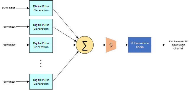
Another approach to the muti-emitter problem is to combine multiple signals within the digital domain. As mentioned earlier, modern wideband vector signal generators are capable of producing digitally-generated IQ signals over a wide bandwidth upconverted to a particular center frequency. Modern VSGs can provide signal bandwidths in the low gigahertz range. Equipped with a wide bandwidth, signals can be simultaneously generated over the source’s bandwidth via digital combination prior to the digital-to-analog converter. In doing so, the architecture can save significantly on RF hardware resources. This is a major advantage when it comes to high density scenarios with many simultaneous emitters being generated. The benefit on the SWAPC improvement cannot be understated. Additionally, the digital combination of signals ensures time alignment at the RF output, assuming each digital baseband generator runs off the same hardware clock.
The drawbacks to the digital baseband combination approach are in contrast to the analog combination benefits. One detail to consider when combining the signals digitally is that each signal is limited by the dynamic range of the digital-to-analog converter (DAC). The single RF front end amplification/attenuation settings increase or decrease the power level of the full wideband signal set accordingly. Independent control of each signal is still made possible via digital attenuation, but the dynamic range is not as robust as the RF front end alone. Additionally, as wider bandwidths are utilized, the SFDR and the noise power within the instantaneous bandwidth will degrade.
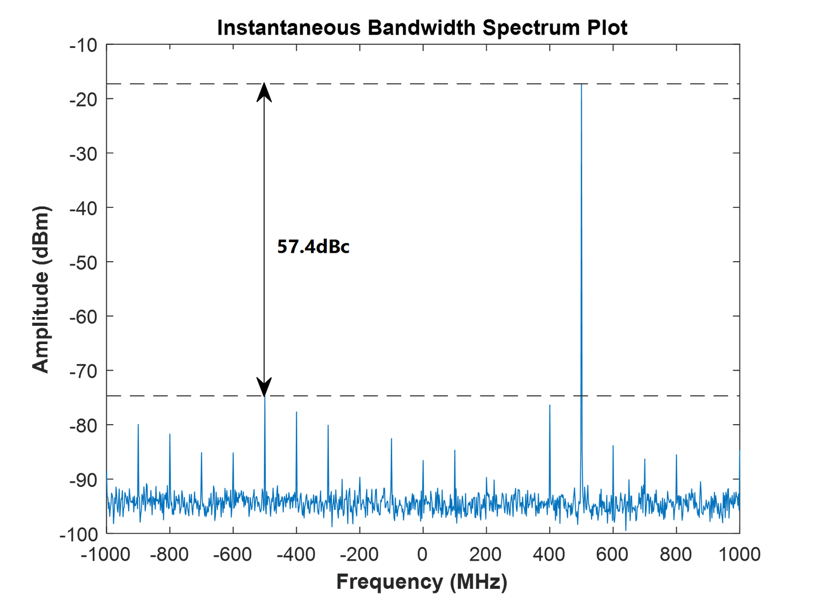
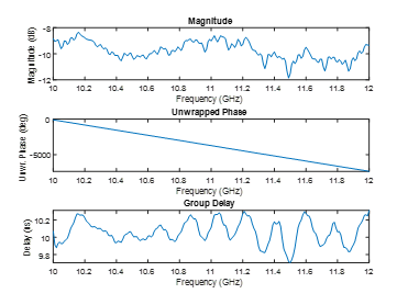
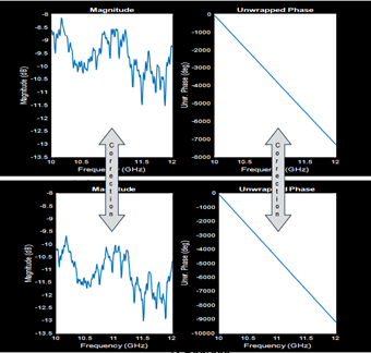
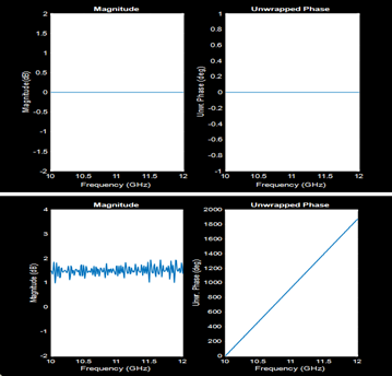
To take a closer look at this phenomenon, consider the following spectral plot of a single emitter signal offset by 500MHz within the instantaneous bandwidth of the VSG. The spurious dBc values are plotted with respect to the carrier signal. In one set of plots, the carrier is attenuated by switching in RF analog attenuation on the source’s front end. In the second set of plots, the carrier signal is digitally attenuated by driving the DAC at lower power levels.
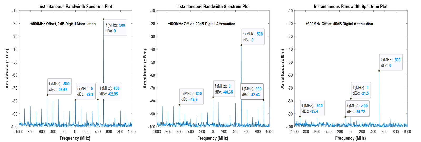
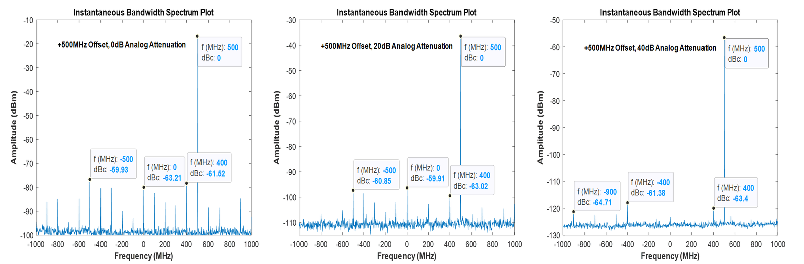
Digital attenuation degrades the SFDR, whereas the analog attenuation does not. Nevertheless, if there were multiple signals spread across the bandwidth the analog attenuation settings would attenuate the full bandwidth, whereas each signal can be controlled digitally. If every signal were combined externally using multiple sources and an RF combiner, the power levels could be controlled independently without degrading the SFDR. Nevertheless, the hardware SWAPC associated with the analog domain combination can quickly become a major issue.
RF Front End with Multi-Port Direction Finding Receivers
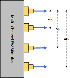
Building upon the discussion around multiple RF emitters, the technical challenge can be expanded by introducing receivers with multiple RF ports for phased-array direction finding capabilities. Phased array technology provides angle-of-arrival (AoA) capabilities to aid in the geolocation of emitters in the environment. In general, AoA can be calculated by measuring the difference in signal phase and/or amplitude between multiple antenna ports, or by measuring the difference in time between pulsed signals arriving at each antenna. A full discussion of EW receiver architectural tradeoffs will not be covered here. This section will describe the process of aligning the timing, amplitude, and phase of multi-port RF signal generation system.
Consider a pulsed RF plane wave emanating from a single source in time and space. Depending on the direction of the plane wave, the amplitude, phase, and time-of-arrival of the pulsed signal will be different on each antenna element of a phased array multi-port receiver. Based on the physical geometry of the antenna elements in the array, the receiver can extrapolate the AoA of the plane wave. To test the receiver, there are two options: 1.) perform an over-the-air test into the antenna array or 2.) stimulate each receiver port with an independent source representing the plane wave at each antenna element, known as direct-inject. The former technique requires a test range and physical geometrical precision. It also requires a source and antenna to be configured per RF emitter. This can become expensive and space limited very quickly depending on the over-the-air test range. The latter technique requires a source per RF port, although not a source per RF emitter as discussed in the section above. This technique mitigates the need to rent time on a test range and time/cost configuring antenna elements.
The direct inject technique requires the simultaneous port stimulation to act as a plane wave in an over-the-air test. To do so, one must understand the concept of aligning RF stimulus ports in timing, amplitude and phase. Consider two RF signals from two different RF sources. The two sources have two independent RF paths including mixers, amplifiers, attenuators, cabling, and more. The two sources may be the same part number from the same vendor, but physical tolerances and environmental conditions will almost never lead to identical frequency responses through each RF source path. One must therefore apply an alignment technique to align the output of both sources in timing, amplitude, and phase.
Think of a single RF source cabled to a single receiver input port. Between the digital-to-analog converter (DAC) and the receiver input there is a distinct frequency response to the RF network.
Now consider two RF sources with two distinct frequency response curves. The goal of port alignment is to null out the discrepancies in frequency response between the two RF ports at the receiver inputs. This can then expand to many RF ports depending on the number of array ports on the receiver.
Taking the difference between the two frequency response curves from the two independent RF source paths provides a mechanism for creating a correction filter. By assigning one source path as the reference path, an FIR filter can be constructed to apply the correction to the secondary path. This filter is commonly referenced as a predistortion filter. The predistortion filter results in an identical frequency response at the input to the two receiver ports.
Measuring the Relative Frequency Response
In theory, collecting the frequency response of each RF stimulus port and applying correction filters is an ideal mechanism for ultimately creating a plane wave at the receiver input. However, in practice this process is not as straightforward. Obtaining the frequency response of the RF network between the DAC input of the signal source and the connecting cable to the receiver input is not easily accessible. The source is usually housed in a chassis without access to each component in the RF chain.
Rather than directly measuring the response of each RF source independently, the alignment process can be simplified by measuring the relative frequency response at each output port. To do so, each independent source must provide an identical stimulus simultaneously at the RF output port. A measurement system must then measure the relative amplitude, phase, and group delay between ports.
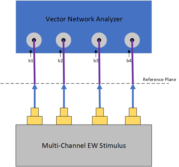
To measure the relative amplitude, phase and group delay between ports there are a series of different measurement devices which could be used. One such setup would be the use of a vector network analyzer (VNA) to do the job. By attaching a VNA port to each independent RF port of the multi-port EW stimulus, the VNA can make relative measurements between its measurement receivers.
VNAs are generally thought of in terms of their S-parameter measurement capabilities. In the case of VNA S-parameter measurements, the VNA provides a single RF source as the input to an RF network. The measurement is made on the relative amplitude and phase values between internal VNA receivers monitoring the source wave and the measured output wave of the RF network. FigureXX provides a diagram of a fundamental VNA architecture.
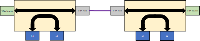
One VNA source is active at any given instant in time. The source drives the input of an RF coupler which feeds power to the VNA port and the “a” receiver internal to the VNA. The source wave travels out of the VNA port and either reflects back toward the driving source or travels through the RF network to the complementary connected port. Waves traveling into either VNA port are captured and measured on the “b” receiver of the VNA. A ratio measurement is made between the “a” reference receiver and the “b” measurement receiver. An SXY measurement indicates the relative measurement made on port Y relative to the reference receiver X from which the source was driven. For example, an S21 measurement measures the port 2 b2 receiver relative to the reference receiver a1 from a source driven on port 1.
In the case of a multi-port EW stimulus source connected to a VNA, the setup deactivates the VNA source and only utilizes the “b” measurement receivers in the VNA. Rather than making relative measurements between reference and measurement receivers, the setup makes relative measurements between b receivers. The figure below shows the multi-port source connected to an independent VNA port. Ratio measurements between the b1 and b2 receivers in the VNA provide the difference in frequency response between RF stimulus ports 1 and 2. Ratio measurements between port 1 and port N will produce the frequency response correction required on port 2 through N to perform plane wave emulation at the receiver input. An FIR predistortion filter can be created on each stimulus port to perform the correction.
To create the test signal for frequency response correction at the EW stimulus port outputs, a specific test signal must be generated to cover the instantaneous bandwidth of the signal source. One such signal could be a digitally generated CW signal swept across the bandwidth. The VNA can be tuned to the specific frequency sweep points across the bandwidth. Instead of sweeping a CW across the band, one could generate a wideband signal which covers the instantaneous bandwidth. In this case, a baseband signal with multiple CW carries spread over the bandwidth would be an ideal test signal to measure the relative amplitude, phase, and group delay.
As the EW stimulus system drives a simultaneous multi-carrier CW signal covering many frequency points over the bandwidth of interest, the VNA b receivers perform ratio amplitude and phase measurements over the swept frequency bandwidth. To measure the time delay between each RF output port, the VNA measures relative group delay over the bandwidth and takes an average value of the delay. Measurement of group delay can be simplified to a relative phase measurement. The relative phase difference between each CW tone can be divided by the frequency spacing between tones to obtain the relative group delay over the bandwidth. The system can then average the group delay over the bandwidth on each port to apply a static delay correction to ports 2 through N.
Upon applying the predistortion filters to correct for phase and amplitude mismatch and by applying the static delays to correct for time delays, each RF port within the system is aligned. This process provides the foundation for plane wave emulation at the reference plane input to the EW receiver.
Local Oscillator Distribution – Maintaining the Alignment
To be able to maintain the reference plane port alignment described in the previous section over long test periods (hours to days), the multi-port system must utilize mechanisms to reduce phase perturbations. As temperature and vibrational variations occur over the test period, minor mechanical variations in physical component length contribute to phase variations at the reference plane of the RF port alignment. One of the most important factors to consider in analyzing the phase stability of an RF system is whether the local oscillator (LO) is distributed to the RF upconverter on each port. This architectural consideration assumes the system has an upconversion stage to reach higher frequencies.
Distribution of the LO provides significant phase stability advantages over the distribution of a lower frequency reference clock source in a PLL-based system. Distribution of a reference clock provides frequency lock, but it does not provide phase coherence between multiple sources. The reference clock, in many architectures, provides a reference to a phase-locked loop (PLL). This reference clock becomes a high frequency RF signal at the output of the PLL’s voltage-controlled oscillator (VCO). For example, a 10MHz reference clock can be converted to a 10GHz LO through a PLL. In this case, one must begin to understand the nature of a PLL. Minor disturbances in the phase at the input to the low frequency PLL reference result in PLL resettling. PLL resettling results in a major phase change at the PLL RF output. In the case of a multi-port signal generation system, this behavior ruins the alignment discussed in the previous section.
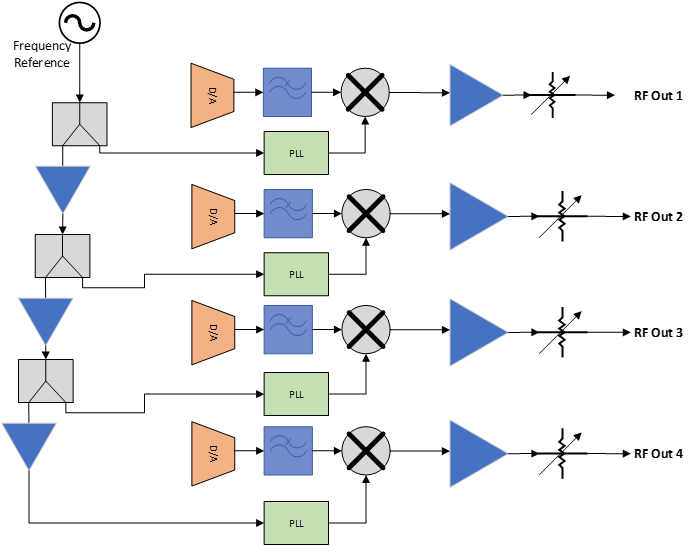
To overcome the challenges of PLL resettling at each signal generation port, the local oscillator of each generator port must be common. Any disturbances in the phase of the common LO will be common across every generator. This behavior maintains the phase alignment between RF ports.
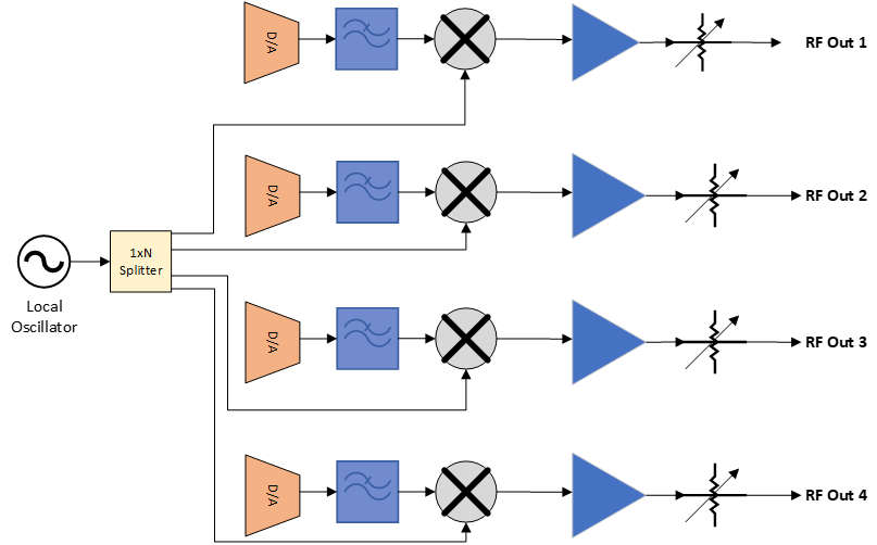
It is important to consider the physical distribution of the common LO to each generator. The LO source should ideally be distributed across common length phase-stable RF cables. Doing so reduces the impact of electrical length discrepancies of the RF network over temperature changes in the test environment. For example, if the temperature increases in the test environment, the mechanical length of identical cables will theoretically fluctuate in the same direction. The common length fluctuation will result in identical phase drift at the generator output ports.
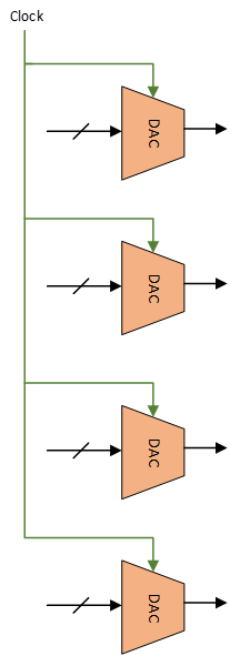
Digital Back End Alignment
In addition to the alignment of the RF generator front end frequency response, it is important to consider the time alignment of the baseband generator driving the digital to analog converter (DAC). The digital back end needs to be utilizing the same clock source to maintain time alignment of the digital signal. Without this feature, signals will begin to drift between ports. Slight timing offsets between DAC clocks can be aligned by shifting the delay in the first IF or IQ sample driving the DAC, but drifting DAC clocks will result in drift of the phase of the RF signal under wideband signal conditions.
Why does the drift more seriously impact the phase of wideband signals? In the case of a narrowband signal, the DAC output is oscillating slowly in time. The DAC is clocked at a higher rate than the slow varying digital signal being driven into the DAC. This slow varying signal does not show a significant phase drift due to the small time difference relative to its wavelength. On the other hand, a higher frequency signal clocked at the same rate will result in much more significant phase drift due to the same amount of time drift.
The effect being described here needs to be considered in the context of the LO frequency as well. If the RF front end LO frequency is much higher than the bandwidth of the digital signal coming from the DAC, the impact of DAC clock drift is not as significant as the frequency response alignment and LO uniformity across the RF front end of the system.